Omron’s Semiconductor Manufacturing: From Front-End Inspection to Finished
January 18, 2024

By Omron Automation
The front-end process of semiconductor manufacturing is critical to quality. As this is when circuits are formed on the surface of the wafer. With semiconductor manufacturing booming in the Americas, fabrication facilities are on the lookout for innovative ways to quickly produce high-quality wafers and gain a competitive advantage. Omron has the solutions to make that happen.
A look at the semiconductor market
An increased demand for consumer electronics, automobiles, medical equipment and devices, data centers, Artificial Intelligence (AI), and the Internet of Things (IoT) are driving increasing demand for semiconductors. This includes commercial, industrial, and defense as cutting-edge development requires specialized chips for their proprietary technology. Collaboration amongst semiconductor fabrication facilities and defense companies is anticipated in the years to come.
Currently, there is a big initiative to increase the production of semiconductors in the United States. The US Federal Government recently launched the CHIPS Act to incentivize the manufacturing of semiconductor chips in the US. Alongside the federal government, state governments are also creating incentives to bring semiconductor manufacturing to their regions as well. Some semiconductor hotspots in the U.S. are the Bay Area, Texas, New England, Arizona, and Minnesota.
Most of the new semiconductor fabrication facilities that are under construction will be manufacturing 300mm wafers. One point of observation is that the fabrication facilities that traditionally produce 200mm wafers are also upgrading their current manufacturing operations as the electric vehicle industry is driving the manufacturing re-birth of 200mm wafers.
Impacts on the semiconductor market
Talent shortages in the industry will accelerate the adoption of industrial automation. According to SEMI, a global association for advancing growth for 3,000 member companies and helping the semiconductor industry deploy lifechanging technologies worldwide, their Fab Owners Alliance Forum from March 2022 predicts that there are over 56,000 job openings in the semiconductor industry in the U.S. They also predict that, by the year 2025, there will be over 300,000 positions related to semiconductor manufacturing in the U.S.1
Increased collaboration between private and academic institutions has the potential to impact the semiconductor industry in the future through talent. U.S. engineering schools are now racing to build the talent pipeline. Universities and community colleges are revamping their semiconductor-related curriculum and are forging strategic partnerships with each other and key industry players to train the staff needed to work in future U.S. semiconductor manufacturing facilities.
Sustainability will continue to have an impact on every industry in the future and semiconductor fabrication facilities will notice an emphasis on waste reduction, energy savings, efficient use of water, and the need to optimize the physical footprint of the manufacturing floor. Semiconductor leaders will continue to implement sustainability roadmaps that will align with their business goals.
Semiconductor manufacturing close-up
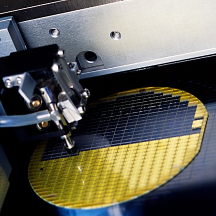
Front-end semiconductor manufacturing, also known as wafer fabrication or wafer processing, is the initial stage in the production of circuits (ICs), and other semiconductor devices. It involves the creation of an integrated circuit on a silicon wafer. The process begins with the preparation of the wafer, which includes cleaning and polishing to ensure a very smooth surface. Front-end wafer manufacturing involves several key processes. First, wafer fabrication begins with the growth of a pure silicon crystal, which is then sliced into thin wafers.
These wafers undergo cleaning, polishing, and doping to create the desired electrical properties based on the downstream consumer’s performance specifications. Next, photolithography is used to pattern the wafer with a photoresist, followed by etching to remove any unwanted material. Multiple layers of transistors, interconnects, and insulators are built using deposition, oxidation, and etching techniques. Finally, wafers undergo testing and inspection to ensure quality before being packaged and sent for back-end assembly and testing.
The time it takes to manufacture a semiconductor wafer can vary depending on several factors, including the complexity of the design, the size of the wafer, and the specific process involved. On average, it can take anywhere from several weeks to several months to complete the entire wafer manufacturing process. This includes steps such as crystal growth, wafer slicing, cleaning, doping, photolithography, etching, deposition, and testing.
Each step requires careful precision and multiple iterations to ensure the desired quality and functionality of the semiconductor wafer as scrap costs and opportunity costs remain high. The most common sizes of semiconductors are 200mm and 300mm wafers. Most of the new fabrication facilities are for 300mm wafers. While the 200mm fabrication was considered legacy, this size is now seeing a resurgence thanks to the rapid adoption of electric vehicles.
Semiconductor manufacturing challenges
Semiconductor manufacturing is not without its challenges. Currently, the number one challenge in the Americas is a shortage of labor. There are dozens of new semiconductor fabrication facilities scheduled to be built, and semiconductor manufacturers are worried about ensuring adequate staff for these new fabrication facilities that will come in line in the next few years. Another challenge the industry is facing is bringing legacy equipment up to date to meet current manufacturing standards. Especially in terms of smart manufacturing, and the leadership of the fabrication is currently evaluating ways to incorporate smart manufacturing standards such as digital twins, predictive maintenance, and data monitoring into their current operations.
To address both these challenges, semiconductor manufacturing facilities are deploying autonomous mobile robots to transport wafers, or working alongside cobots to handle fabrication, or increasing the use of RFID barcode readers and machine vision cameras to ensure full supply chain traceability, or a combination of these strategies.
At the tool level, increasing the sensing capabilities will allow fabrication managers to reduce downtime while meeting very aggressive production demands. Embracing highly precise measuring devices and pairing this with robust controls will allow these managers to identify defects early in the process and capture data to enable better, faster decisions. Where there is precision and automation, Omron’s Sysmac has a track record of delivering value through the holistic control of automation software, motion, and vision.
Enabling technologies for semiconductor manufacturing
Omron Automation has 90 years of experience leading the way in automation and innovation. Their portfolio of products enables semiconductor manufacturers to succeed in this industry. Some examples of these technologies are Sysmac Studio Software, 1S Drive motion, and Microhawk vision.
More Information
Learn more about enabling technologies for semiconductor manufacturing
Related Story
Why Omron’s New SECS/GEM-Complaint Solutions Are Beneficial for Semiconductor Manufacturers
Developed by the non-profit Semiconductor Equipment and Materials International (SEMI), the SECS/GEM connectivity standard is an equipment interface protocol for equipment-to-host data communications that is top-of-mind for many semiconductor manufacturers today.
As a trusted partner in automation solutions for the semiconductor industry, Omron is committed to providing highly innovative technologies that also meet SECS/GEM requirements. Omron takes a look at the purpose behind SECS/GEM and the ways in which these solutions will benefit semiconductor manufacturers.